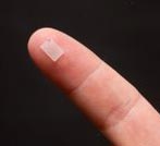
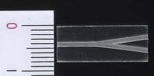
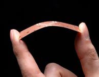
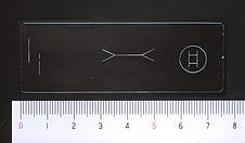
Besides the PCB, MITS have a proven track record of achieving the fine processing thinner than 100µm on the surface of many materials as following;
- Silicon wafer
- Strontium titanate (100)
- Acrylic
- Glass
These processing consist of a lot of know-how, such as “stepping process technology” in Z-axis
 |
 |
|
Silicon wafer
|
Strontium titanate (100)
|
 |
 |
|
Acrylic
|
Even on the extremely thin circuit board
|
 |
|
| Glass material | Magnified picture |